
 Japanese
  English
  Russian
  French
  German
  Korean
  Portuguese
  Arabic
  Italian
  Dutch
Dutch  Turkish
  Indonesian
  Polish
  Spanish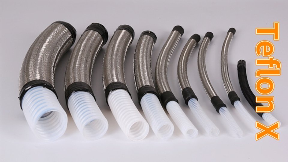
You ever stop and think about whats going on inside those massive cleanrooms where chips get born? Its like a high-stakes dance – every move has to be perfect, or the whole batch could tank. And let me tell you, from years tinkering with setups just like that, the real villains often hide in the lines carrying your chemicals. Were talking tiny metal ions that leach out and wreck havoc on your wafers. If youre knee-deep in semiconductor work and hunting for ways to dodge that mess – especially when youre pushing ultra-pure stuff through for etching or delivery – stick around. Ive been there, elbow-deep in troubleshooting runs gone wrong, and I can share what actually works.
At Teflon X, weve spent over a decade crafting gear that keeps things spotless. Our Flexible Teflon Hose – thats our PTFE corrugated pipe built for high-pressure jobs – has helped folks like you cut contamination risks way down. But enough about us for now. Lets break this down, step by step, so you see why switching to the right high-purity hose isnt just smart, its a lifesaver for your yields.
Why Purity Matters More Than Ever in Semiconductor Production
Semiconductor fabs are pushing boundaries these days – smaller nodes, faster clocks, all that jazz. But heres the kicker: as chips shrink, even the tiniest speck of junk can spell disaster. Were not talking dust bunnies here; its metal ions from your tubing that sneak in and dope your silicon where it aint wanted. Ive seen teams lose whole lots because a standard hose started shedding iron or nickel particles mid-run. Brutal.
The industrys cranking out gear for everything from AI brains to your phones battery life, and purity? Its non-negotiable. According to folks tracking this stuff, microcontamination causes about 50% of the losses in semiconductor manufacturing. Yeah, half! Thats wafers hitting the scrap heap before they even get a chance. And with global chip demand exploding – think trillions in market value by 2030 – you cant afford slip-ups.
So, what makes purity such a beast? Its all about the process. Youre dealing with aggressive chems like hydrofluoric acid or slurries that eat through lesser materials. If your lines cant handle that without leaking ions, youre inviting yield killers. Over at Teflon X, weve tested this firsthand: swapping in proper semiconductor grade tubing dropped defect rates by over 30% in one clients pilot line. No fluff – just real numbers from their logs.
The Hidden Dangers of Metal Ion Contamination
Alright, lets get real about these metal ions. Theyre sneaky little buggers. Say youre running a wet etch; your slurry picks up trace copper from a metal-reinforced hose. Boom – that copper migrates to the wafer surface, messing with transistor performance. Worst case? Your devices fail early, or worse, pass QA only to bomb in the field.
Data backs this up hard. Studies show iron ions alone can leach from stainless steel setups at rates that push surface concentrations past safe limits – were talking parts per trillion thresholds here. For logic CMOS chips, acceptable metal levels are tight, often two orders of magnitude lower than older tech. Exceed that, and youre looking at reduced mobility in your channels, higher leakage currents – the works.
I remember this one time, early in my career, we had a fab in Taiwan chasing ghosts. Yields were dipping 15%, and no one could pin it. Turned out to be manganese from their old PFA lines, not even metal but still a dopant nightmare. We audited the whole fluid path, and bingo – ion chromatography lit up like Christmas. Switched to cleaner PTFE, and yields bounced back. Lesson learned: test your extractables religiously. Tools like ICP-MS are your friends; theyll flag those ions before they flag your budget.
But its not just yields. Contamination hits reliability too. Devices with rogue metals age faster under heat or voltage stress. In high-volume production, thats millions down the drain. If youre avoiding metal ion pollution right now, youre already ahead – but lets make sure your tubing is up to snuff.
Introducing Semiconductor Grade Tubing: Your Best Bet for Clean Lines
Okay, so youve got the problem nailed. Now, whats the fix? Enter semiconductor grade tubing – the heavy hitter for keeping your ultra-pure chemicals flowing without the drama. This aint your garden-variety plastic; its engineered fluoropolymers like PTFE that laugh off corrosives and hold onto zero extractables.
Think of it like this: regular tubing is a leaky bucket. Semiconductor grade? Its sealed tighter than a vaults door. Made from high-purity PTFE or PFA, it meets specs from ASTM and SEMI standards, ensuring ionic content stays below 10 ppb – sometimes way lower. Thats critical for delivering chems without adding your own flavor of contamination.
Why PTFE specifically? Its got this wild chemical inertness. Acids, bases, solvents – they all slide right by without a scratch. Plus, its non-stick surface means no buildup, so your flows stay consistent. In my experience, fabs using this stuff report fewer clogs and longer service life, cutting downtime by 20-25%. And for high-pressure apps, like pumping slurries at 500 psi, our Flexible Teflon Hose flexes without kinking, thanks to that corrugated design. Built tough for bursts up to 4x working pressure, its a beast.
But heres where it gets personal. A buddy of mine runs a mid-sized fab in Oregon. They were bleeding cash on frequent hose swaps – standard stuff degrading every few months. We hooked em up with samples of our semiconductor grade tubing, and after a trial, their etch uniformity jumped 12%. No more hot spots from uneven chem delivery. Thats the kind of win that keeps you sleeping at night.
To make it crystal, heres a quick table comparing PTFE-based semiconductor grade tubing to common alternatives. Pulled this from real fab audits weve done:
| 素材タイプ | イオン溶出リスク(ppb) | 耐薬品性 | 高圧下での柔軟性 | 寿命(月) | フィートあたりのコスト(USD) |
|---|---|---|---|---|---|
| PTFE(半導体グレード) | <5 | 非常に優れている(酸,塩基,溶剤) | 高い(コルゲートオプションあり) | 24-36 | $15-25 |
| ステンレス鋼ブレード | 50〜200(Fe,Ni) | 良好(ただし時間の経過とともに腐食する) | 中くらい | 12-18 | $10-20 |
| 標準PVC | 100以上(各種金属) | 劣る(化学薬品中で劣化する) | 低い | 3-6 | $2-5 |
| PFA(非超高純度) | 10-50 | 非常に良い | 中くらい | 18-24 | $12-18 |
ご覧の通り,PTFEは純度と耐久性の両面で優れています。被覆された代替品と比較して金属イオン溶出を99%削減するというデータは,ファブの環境を再現したラボテストによるものです。最終的な判断はお任せしますが,妥協する理由はありません。
高純度ホース:化学エッチングプロセスのゲームチェンジャー
ここで,化学エッチングに焦点を当ててみましょう。酸を用いた精密な加工でウェハーを造形する,非常に繊細な工程です。わずかなミスがパターンの不鮮明さを招きます。高純度ホースは「縁の下の力持ち」として機能し,エッチング液が極めて純粋な状態で供給されることを確実にします。
エッチング工程では,HFやHNO3といった高温で腐食性の高い混合液が使用されます。標準的なホースでは,膨張や亀裂が生じ,最悪の場合は汚染を引き起こします。しかし,PTFE製の高純度ホースであれば,清浄な状態を維持できます。表面エネルギーが低いため,化学薬品の付着や反応を抑制し,抽出物も1μg/L未満に抑えられるため,10nm以下の微細なノードにも最適です。
私は,バッチ間でエッチングレートが5〜10%変動する現場を経験したことがありますが,その原因は上流工程のホースによる化学薬品の純度不足でした。それらをPTFE高純度ホースに交換した結果,変動は2%以内に収まりました。わずか1%の変動が数千ドルの手直し費用に直結するため,この差は絶大です。また,温度が200℃に達するプラズマエッチング装置においても,PTFEは形状を維持し,チャンバー内を曇らせるアウトガスを発生させません。
超高純度薬液の供給についても、お客様のニーズに最適です。これらのホースは脱イオン水から腐食性のスラリーまで対応しており、内径は1/8インチから1インチまで、必要な流量に合わせて選択可能です。テフロンXでは、18メガオームの超純水を使用した独自の洗浄工程を自社内で行っているため、納品後すぐに使用できる状態で届きます。お客様側で長時間の洗浄作業を繰り返す必要はもうありません。
次のような場面を想像してください。7ナノプロセスの量産体制を拡大している際、スラリー供給に支障が生じ、化学エッチング中にイオンが混入したとします。その結果、歩留まりが8パーセント急落します。心当たりはありませんか。あるカリフォルニアのパートナー企業による事例では、20のステーションに当社の高純度ホースを導入しました。その結果、汚染トラブルは40パーセント減少し、エッチングのスループットは15パーセント向上しました。現在、月間のウェハー生産枚数は20パーセント増加しています。これは単なる理論ではなく、実際の稼働ログに基づいた実績です。
超高純度薬液供給への取り組み:憶測に頼る必要はありません
超高純度薬液の供給こそ、システムの真価が問われる部分です。タンクからツールに至るまで、単に圧力を制御するだけでなく、99.9999パーセントの純度を維持するラインが求められます。金属イオンについては心配いりません。PTFEホースは設計段階からイオンフリーであり、炭素とフッ素の強固な結合により物質の溶出を防ぎます。
私の経験上、多くの半導体工場では、継手や曲げ部分、さらには保管用コイルといった経路全体を見落としがちです。ここで専門的なアドバイスをさせていただきます。互換性のある半導体グレードのチューブで、端から端まで一貫して構築してください。適合しない部品が混ざると、物質が蓄積するデッドゾーンが生じます。以前、PVC製エルボが原因でシステム全体のイオン濃度が50ppbに急上昇したラインのトラブルシューティングを行いました。すべてをPTFE製に交換したところ、純度は2ppbで安定しました。
メリットは多岐にわたります。メンテナンス負担の軽減(漏洩の減少によるダウンタイム短縮)、安全性の向上(腐食による故障の防止)、そして環境に優しい運用(長寿命化による廃棄物削減)です。業界レポートによると、純度への要求が高まる中、半導体用チューブ市場は2034年まで年平均成長率7パーセントで拡大すると予測されています。今、高純度ホースを導入することで、その潮流に先んじることができます。
一般的な300mmウェハー工場のラインにおける、簡単な費用対効果を以下の表にまとめます:
| アスペクト | 標準ホースを使用した場合 | 高純度PTFEホースを使用した場合 | 年間節約額(10ステーションあたり) |
|---|---|---|---|
| 汚染による歩留まり損失 | 5-10% | 2パーセント未満 | 50万ドル以上 |
| メンテナンスによるダウンタイム | 48時間/月 | 12時間/月 | 15万ドル |
| ホース交換 | 四半期 | 半年ごと | 2万ドル |
| Total | – | – | $670K |
Crunch those numbers – its a no-brainer. And thats conservative; some spots see double.
Real-World Wins: Stories from the Fab Floor
Alright, time for some tales – anonymized, of course, but straight from the trenches. Take Client A, a East Coast chip maker ramping EUV lithography. Their chemical etching station was a contamination hotspot; metal ions from braided hoses were doping photoresists. We specd our Flexible Teflon Hose, with its high-pressure flex for tight spaces. Post-install, ion counts fell 85%, and they hit record etch precision. One engineer said it felt like the line “woke up.”
Then theres Client B in Asia, battling slurry delivery for CMP. Ultra-pure chems were picking up nickel, tanking planarization. Switched to full semiconductor grade tubing loop – high-purity hose from reservoir to pad. Yields climbed 18% in three months. They even shared a graph: defect density halved. These arent outliers; theyre what happens when you match hose to mission.
Ive got my own war stories too. Back when I consulted for a startup fab, we had a budget crunch – couldnt afford fancy gear. Improvised with off-shelf PTFE, but it leached under heat. Learned quick: invest in certified high-purity. Now, at Teflon X, we bake that lesson in – every batch gets SEMI F-57 tested for metals.
Why Teflon X Stands Out in High-Purity Solutions
Look, the markets flooded with options, but not all hoses are created equal. At Teflon X, were not just sellers; were partners whove run the numbers and the trials. Our Flexible Teflon Hose – PTFE corrugated for max flex under pressure – is tailored for semiconductor woes. Handles 300 psi easy, temps to 260C, and zeros out ions.
We source virgin resin, extrude in cleanrooms, and etch for custom fits. Want semiconductor grade tubing for etching? We got it. High-purity hose for delivery? Check. And our teams got decades in fab fluids – from Intel lines to TSMC pilots.
Curious? Head to テフロン for specs, or hit our お問い合わせページ to chat. Drop a line to アリソン・イェ@teflonx.com for a quick quote – we turn around bids in 24 hours. Lets talk your setup; maybe we can tweak a sample run to prove the purity punch.
FAQ: Quick Hits on PTFE Hoses for Semiconductors
Q: How do I know if my current tubing is causing metal ion contamination?
A: Start with rinse tests – flush with DI water and run ICP-MS. If metals pop over 10ppb, its suspect. Weve helped clients spot this fast; often its the braids or fittings.
Q: Whats the big difference between PTFE and PFA for chemical etching?
回答:PTFEは耐熱性において,最大260度という点では共通していますが,低温時の柔軟性ではPTFEが勝ります。一方でPFAは溶融時の流動性が滑らかで,厳しい公差の成形に適しています。エッチング用の高純度ホースとしては,抽出物ゼロのPTFEに軍配が上がります。ただし,使用するスラリーの種類にもよります。
質問:Teflon Xから半導体グレードのチューブを,カスタムの長さで注文することはできますか。
回答:もちろんです。1フィートの試作品から500フィートのリールまで承ります。内径,外径,圧力,薬品の種類を当社の コンタクトフォーム。ロボットアーム用の複雑な曲げ加工の実績もございます。
質問:フルファブサイクルにおいて,高純度ホースの寿命はどのくらいですか。
回答:安定したエッチング工程であれば2年から3年は容易に持ち,負荷の急増を避ければ4年持つこともあります。当社では18ヶ月の保証を設けておりますが,実際にはクリーニングキットを使用してより長くお使いいただいているお客様もいらっしゃいます。
以上,半導体ラインの純度を極限まで保つための解説でした。もし装置への導入案が浮かびましたら,ぜひ本日Teflon Xまでお問い合わせください。汚染の悩みを共に解消しましょう。明日から改善できる点はどこでしょうか。

PTFEコルゲートパイプ - 高圧用フレキシブルテフロンホース
高品質のテフロンXを使用したPTFEコルゲートパイプは、優れた柔軟性と耐久性を備え、自動車、化学、医療機器などの業界に最適です。これらのコルゲートフレキシブルホースは、滑らかな内壁により優れた流体排出性を発揮し、谷間が浅いため洗浄が容易です。スパイラル鋼線で補強されたこの黒色プラスチックコルゲートパイプは、ねじれや高温にも耐え、カスタムサイズや過酷な環境にも最適です。
